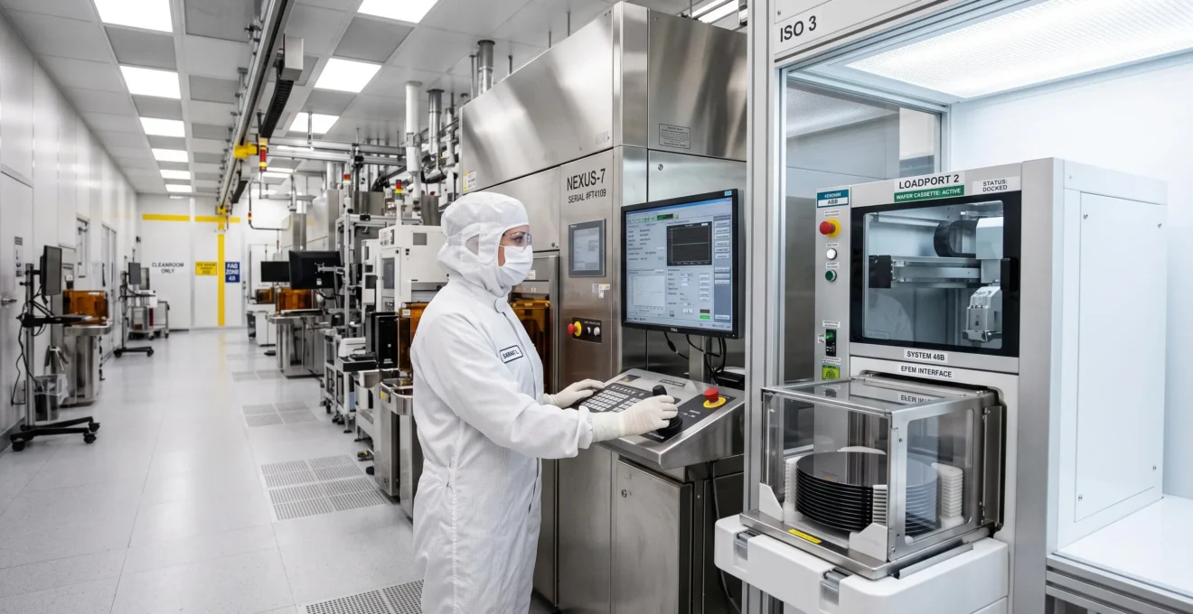
Semiconductor fabrication transforms raw silicon into the microprocessors and memory chips powering modern technology. That transformation unfolds across four major processing stages, each demanding atomic-level precision and contamination-free environments that make cleanroom surgery look casual by comparison.
The journey from silicon crystal to functional chip spans six to eight weeks, involves up to 1,400 individual process steps, and requires wafers to pass through the same equipment dozens of times. Understanding these four stages reveals how advanced automation enables repeatable nanometre-scale precision.
Your semiconductor fabrication workflow in four essential stages
- Wafer Preparation: purified silicon crystals sliced into ultra-flat, contamination-free substrates
- Thin Film Deposition: atomic-layer precision builds insulating and conductive layers using CVD/PVD/ALD
- Photolithography & Patterning: light-based printing creates nanoscale circuit designs (repeated 20-50 times per wafer)
- Doping & Metallisation: ion implantation activates electrical properties, interconnects complete functional circuits
Crystal Perfection: Engineering the Silicon Canvas
Before any circuit patterns emerge, semiconductor fabrication begins with creating the substrate itself—a silicon wafer of extraordinary purity and crystalline perfection. This purity threshold is formally described in the silicon ingot production application note, which documents how silicon undergoes multiple distillations to reach 99.9999999% purity, known in industry specifications as 9N grade.
99.9999999%
(9N purity)
Silicon wafers demand extreme purity—imperfections at the atomic level cascade into defects across all subsequent processing stages, directly impacting yield
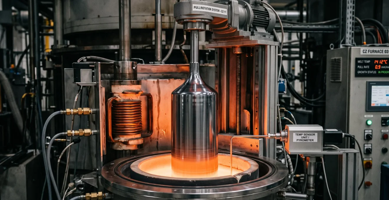
The Czochralski crystal-pulling technique dominates industrial silicon production. A seed crystal touches molten silicon at 1400°C+, then slowly withdraws whilst rotating, solidifying into a single-crystal ingot grown to 300mm diameter for advanced fabs. Diamond saws slice this ingot into 0.7mm-thick wafers, then chemical-mechanical polishing achieves mirror-like flatness essential for nanoscale processing. Any crystalline imperfection or surface contamination here multiplies through every subsequent layer.
Atom by Atom: How Thin Films Shape Functionality
With pristine wafers prepared, fabrication moves to building the functional layers that will eventually form transistors, capacitors, and interconnects. Thin film deposition processes add insulating and conductive materials in precisely controlled thicknesses ranging from a few nanometres to several micrometres, depending on the layer’s electrical function.
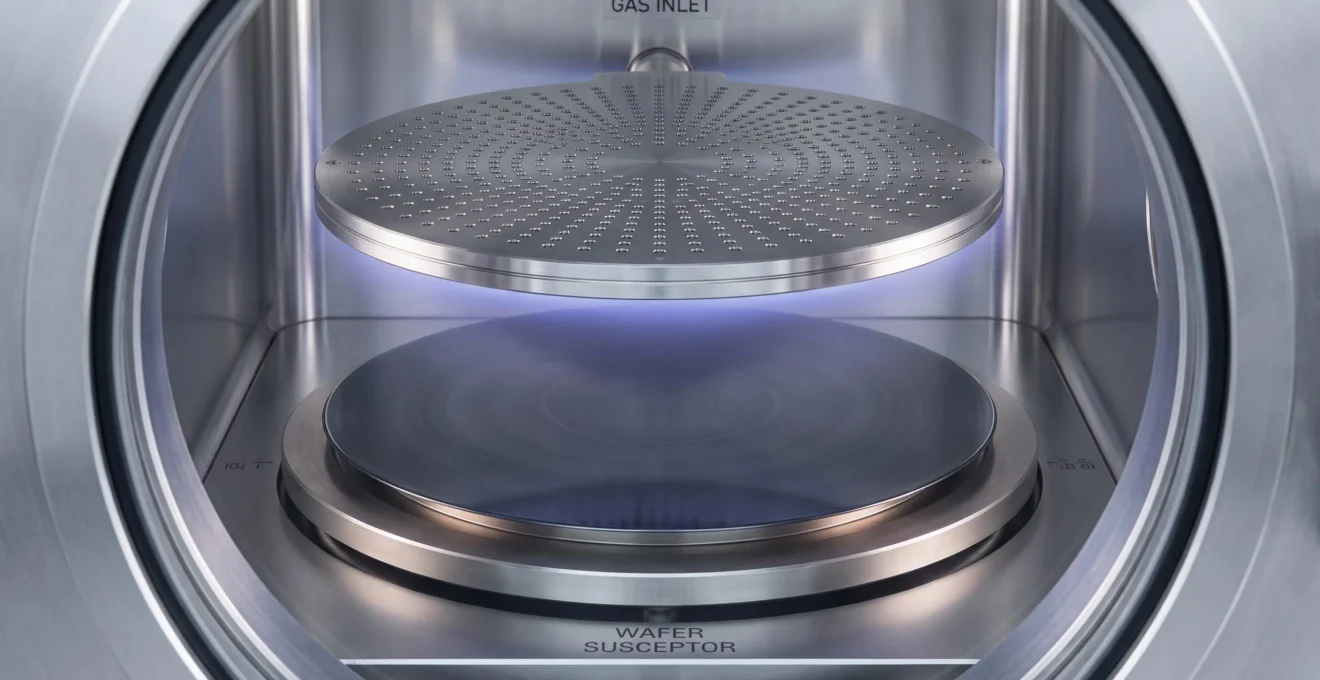
Three primary deposition technologies dominate modern fabs. Chemical Vapour Deposition (CVD) flows precursor gases over heated wafers, depositing films for silicon dioxide insulators and polysilicon gates. Physical Vapour Deposition (PVD) employs high-energy sputtering for metal films. Atomic Layer Deposition (ALD) builds films one atomic layer at a time, achieving unmatched thickness uniformity.
Equipment uptime protects wafer integrity: Automated wafer handling systems (EFEM, loadports, robots) orchestrate thousands of contamination-free transfers daily. A single equipment failure during deposition cycles can expose wafers to particulates, compromising entire batches. Maintaining precision and uptime across this automated handling infrastructure requires specialised expertise—modern fabs increasingly partner with semi-conductor production machine reconditioning department services to restore equipment to OEM specifications and minimise contamination-risk downtime.
Film deposition operates within sealed chambers where atmosphere, temperature, and pressure reach pharmaceutical-grade precision. Maintaining uniform thickness across the wafer surface proves critical—variations exceeding a few percent cause electrical performance mismatches. Advanced fabs monitor film growth in real time and adjust process parameters dynamically.
Light as a Chisel: Carving Nanoscale Patterns
Photolithography transforms deposited films into functional circuit patterns at nanometre scales. Light-sensitive photoresist coats the wafer, then ultraviolet light shines through a patterned mask, exposing specific regions. Chemical developers remove exposed or unexposed resist, leaving a protective pattern. Subsequent etching transfers the mask design into the underlying material.
Photolithography isn’t just the most time-intensive stage—it’s the precision bottleneck that determines whether you achieve target yields at advanced nodes. Alignment accuracy below 2 nanometres and dose control within 1% are non-negotiable.
Dr. Sarah Chen, Process Engineer specialising in EUV lithography
Affirmation: The 4 stages occur in a clean, linear sequence from start to finish
Réponse: Modern semiconductor fabrication involves 20-50 repeated cycles of photolithography, etching, and deposition. A single wafer passes through the same equipment dozens of times to build multi-layer structures. This iterative reality explains why manufacturing a finished semiconductor wafer takes about 12 weeks on average, with advanced processes extending to 14-20 weeks. This demonstrates why quality control remains the cornerstone of manufacturing excellence—semiconductor fabs operate at the extreme end of the tolerance spectrum.
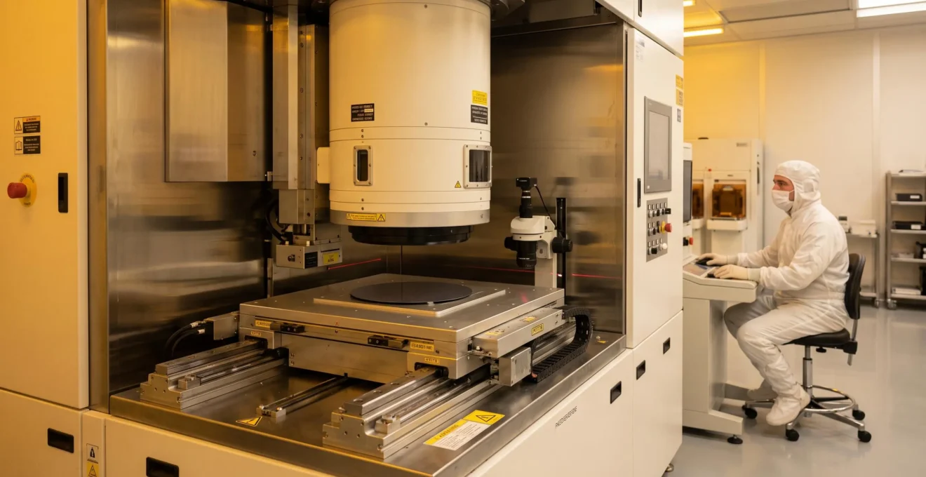
Industry trends increasingly favour Extreme Ultraviolet (EUV) lithography for sub-7nm nodes. EUV employs 13.5nm wavelength light—14 times shorter than conventional deep-UV—enabling sub-wavelength feature resolution. Steppers and scanners achieve positional accuracy in fractions of a nanometre, with overlay tolerances tighter than a silicon atom’s width.
Electrical Awakening: From Inert Silicon to Active Circuits
Patterned silicon remains electrically inert until doping introduces controlled impurities. Ion implantation accelerates dopant atoms (boron, phosphorus, or arsenic) to high energies, embedding them at precise depths. Boron creates P-type regions whilst phosphorus generates N-type regions—the fundamental building blocks of transistors.
Thermal annealing cycles following implantation repair crystal damage and electrically activate dopants. This thermal budget becomes a delicate balancing act—insufficient annealing leaves dopants inactive, whilst excessive heat causes unwanted diffusion that blurs concentration profiles essential for nanometre-scale transistors.
Metallisation creates conductive interconnects wiring billions of transistors into functional circuits. Modern chips employ copper interconnects in low-k dielectric insulators, arranged in up to fifteen stacked metal layers. Each layer requires deposition, photolithography patterning, and chemical-mechanical polishing before adding the next level.
Testing and packaging complete the transformation. Electrical probe testing checks each die, identifying defects. Surviving dies are diced and mounted into protective packages. Global semiconductor manufacturing capacity continues expanding, enabled by automation and precision control throughout these four stages.
These four stages—wafer preparation, thin film deposition, photolithography, and doping with metallisation—represent a deceptively simple framework for one of humanity’s most intricate manufacturing achievements. Each stage repeats dozens of times with atomic-level precision, orchestrated by automation systems moving wafers through kilometres of equipment without human contact.
Understanding this workflow reveals why semiconductor fabs rank among the most capital-intensive facilities on Earth, and why fully automated wafer handling became essential for survival. The nanometre precision demanded by current nodes cannot tolerate human intervention’s inherent variability and contamination risk.